
IIT Guwahati, Columbia University develop optical driving process to produce nanopatterns

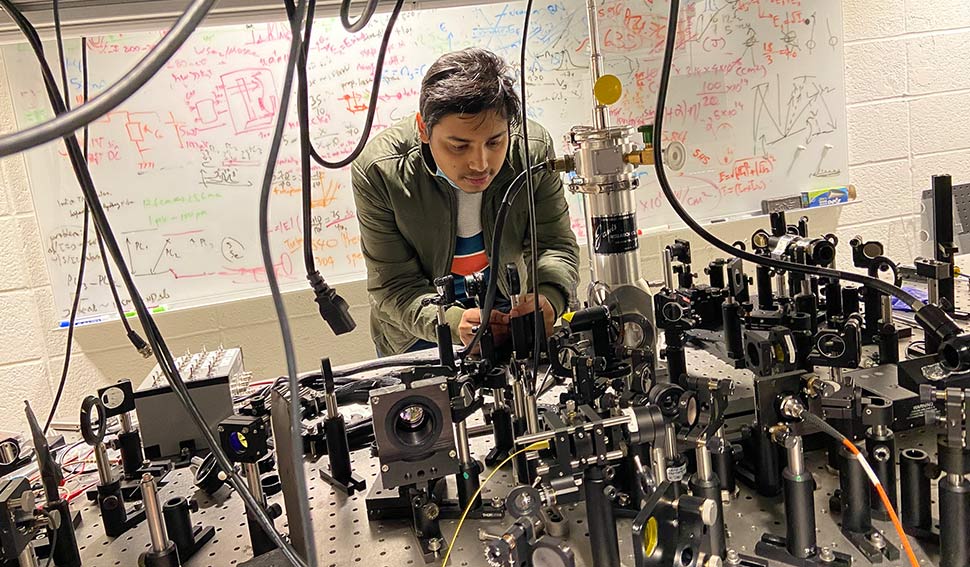
Researchers from Indian Institute of Technology (IITG) Guwahati and scientists from Columbia University, USA have developed a groundbreaking method for nanopatterning using a simple tabletop IR laser.
Dr Rishi Maiti, Assistant Professor at the Department of Physics at IIT Guwahati, formerly a post-doctoral scientist from Alexander Gaeta’s quantum and non-linear photonics group, has published the findings of this research in the prestigious journal, Science Advances.
Nanopatterning involves creating patterns on materials at the nanometer scale, which is a hundred thousand times smaller than the width of a single human hair. This technique enables the fabrication of nano-scaled optical elements and polariton cavities, crucial for devices such as advanced light detectors, solar cells, lasers, and light-emitting diodes.
Traditional nanoscale patterning methods require specialized equipment and infrastructure, such as clean rooms for electron beam lithography machines, or techniques involving high local heating and plasma due to the direct writing. In search of a more accessible and cost-effective alternative, the multi-institutional team adopted a less strenuous process called “optical driving,” leveraging the resonance frequency principle in materials.

By employing this technique, termed “unzipping,” the researchers were able to cleave hexagonal boron nitride using an infrared laser. This resulted in the formation of atomically sharp lines across the sample, measuring just a few nanometers in width. Laser wavelengths at 7.3 micrometres facilitated clean lattice breaks, yielding controllable nanostructures.
Subsequently, the researchers “unzipped” two parallel lines, creating a nano-dimensional cavity capable of trapping phonon-polaritons, unique quasi-particles formed from the interaction of light and vibrations. These trapped particles have the potential to concentrate light into sub-nanometric spots, which could be beneficial for highly sensitive mid-infrared sensing and spectroscopy.
Dr Rishi Maiti said, “This novel nano-patterning technique using optically induced strain opens doors to a myriad of possibilities in nanoscience and technology. Its simplicity and effectiveness mark a significant advancement in the field, with far-reaching implications across various industries.”
Dr Maiti envisions diverse applications for this breakthrough, including designing hard masks for electrode fabrication on 2D materials and forming twisted heterostructures for quantum technologies.


Leave a Reply